Tokyo Ohka Kogyo Product Site
Redistribution Layer (RDL) Resist

Photoresist for Redistribution Layer (RDL) Plating
We offer a wide range of resists for rewiring and plating applications, covering film thicknesses from thin to thick layers of 2–20 µm.
Our resists feature high resolution and a wide depth-of-focus (DOF) margin, enabling advanced high-density semiconductor packaging technologies such as 2.5D/3D semiconductor packaging, TSV (Through-Silicon Via) stacked memory, WL-CSP (Wafer Level Chip Scale Package), FOWLP/FOPLP (Fan-Out Wafer-/Panel-Level Package), and the formation of fine RDLs on silicon interposers.
We provide high-resolution chemical amplification type resists.
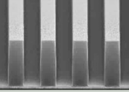
PMER P-BZ Series
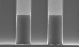
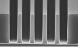
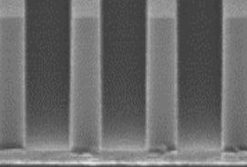
This is a photoresist for RDL formation for thick films of 8~20μm. A rectangular shape can be obtained even in thick film areas.
Features
- Positive-tone type
- Developer:TMAH 2.38%
- Resist film thickness: 8〜20μm
- Wide process margin, good removability
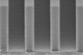
Resist Pattern Shape
| L/S | 10μm/10μm | 8μm/8μm | 6μm/6μm | 4μm/4μm |
|---|---|---|---|---|
| Resist Thickness 20μm |
 |
 |
 |
 |
Conditions
Substrate
Cu
P.A.B.
140℃, 330sec
Exposure
g-, h-, i-line stepper (NA: 0.18)
P.E.B.
100℃, 180sec
Development
TMAH 2.38%,
60sec x 2 paddles
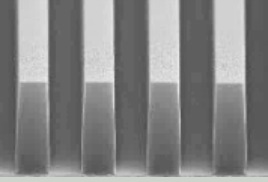
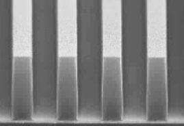
PMER P-CM Series
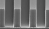
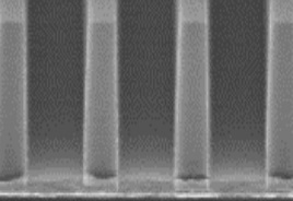
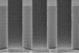
This series of photoresist for ultra-high resolution RDL formation, which is used to form 1.5μm patterns, has an extremely wide defocus margin and good plating solution resistance.
Features
- Positive-tone type
- Developer:TMAH 2.38%
- Resist film thickness:3〜12μm
- High resolution, wide DOF margin, and good removability
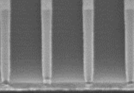
Resist Profile
| L/S | 2μm/2μm | 1.0μm/1.0μm |
|---|---|---|
| Resist Thickness 5μm | 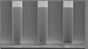 |
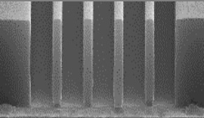 |
DOF Margin
| Resist Thickness 6μm Center 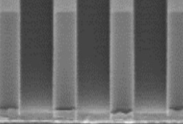 |
+4μm | +8μm | +12μm |
|---|---|---|---|
 |
 |
 |
|
| -4μm | -8μm | -12μm | |
 |
 |
 |
Conditions
Substrate
Cu
P.A.B.
130℃, 300sec
Exposure
i-line stepper (NA: 0.18), 180mJ/cm2
P.E.B.
100℃, 90sec
Development
TMAH 2.38%,
30sec x 2 paddles
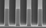
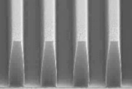
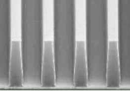
PMER P-WT Series
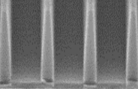
This series of photoresist for ultra-high resolution RDL formation, which is used to form 1.5μm patterns, has an extremely wide defocus margin and good plating solution resistance.
Features
- Positive-tone type
- Developer:TMAH 2.38%
- Resist film thickness:3〜12μm
- High resolution, wide DOF margin
- Compatible with both i-line and h-line wavelengths
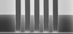
Resist Profile
| L/S | 2μm/2μm | 1.5μm/1.5μm |
|---|---|---|
| Resist Thickness 6μm | 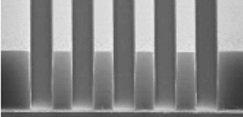 |
 |
DOF Margin
| Resist Thickness 6μm Center 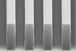 |
+4μm | +8μm | +12μm |
|---|---|---|---|
 |
 |
 |
|
| -4μm | -8μm | -12μm | |
 |
 |
 |
Conditions
Substrate
Cu
P.A.B.
130℃, 300sec
Exposure
i-line stepper (NA: 0.18), 220mJ/cm2
P.E.B.
90℃, 240sec
Development
TMAH 2.38%,
30sec x 3 paddles
Please Feel Free to Contact Us for More Information
For any questions or concerns,
Send an Inquiry Through the Web
Contact Us/Download Information
Please contact us if you have any requests or problems.
You can also access information related to each product.