Tokyo Ohka Kogyo Product Site
Bump Formation Resist
Resist for Photobumping for Copper, Tin, Nickel and Solder Electrolytic Plating such as Au Bumping, Cu Pillar and Microbumping
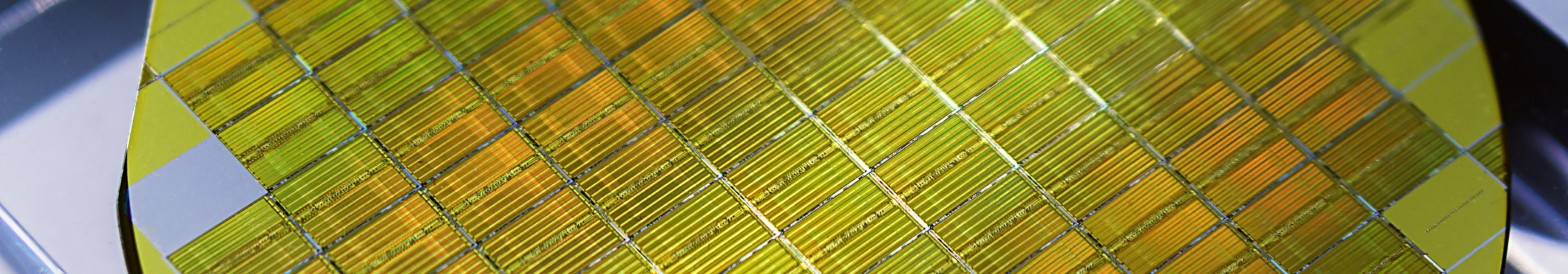
This is a high-resolution, positive-tone thick photoresist for electroplating applications, designed to provide excellent resistance to a wide range of metal plating solutions, including non-cyanide gold, silver, tin, copper, and nickel.It is widely used for electrode formation in advanced high-density semiconductor packaging technologies, such as 2.5D/3D through-silicon via (TSV) packages, stacked TSV memory, wafer-level chip-scale packages (WL-CSP), Cu pillar and flip-chip packages, as well as microbumps, gold stud bumps, and Cu posts for LCD driver applications.
The resist enables fine hole pattern formation with high sensitivity and offers strong adhesion to underlying substrates, providing a wide process margin during electroplating.In addition, compared with negative-tone resists, the resist film can be removed more easily after the plating process, contributing to cost reduction in bump electrode formation processes.A wide range of resist thicknesses from 10 to 100 µm is available to meet various process requirements.
We also offer a comprehensive lineup of process materials compatible with advanced semiconductor packaging technologies such as SiP (System in Package) and PoP (Package on Package).
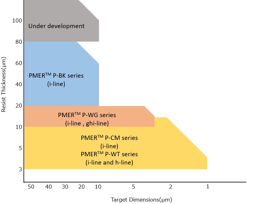
Electrolytic Plating Photoresist Lineup
Photoresist for Cu Pillars and Microbumps
Cu Pillar Bump, Sn/Ag Bump, Microbump Formation

PMER P-BK Series
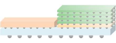
This is a positive-tone photoresist for electroplating processes, offering high resolution and excellent resistance to plating solutions.It is suitable for high-aspect-ratio electroplated electrode formation processes required for applications such as Cu pillar BGA and TSV memory microbumps.The resist supports continuous electroplating of Cu, Ni, and SnAg.In addition, it provides good stripping performance after the electroplating process, allowing the resist to be easily removed without causing damage to the electrodes.
Features
- Positive tone type
- Developer: TMAH 2.38%
- Resist film thickness: 20µm〜65µm
- Wide process margin & crack margin
- Rectangular shape & good removability
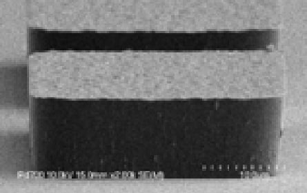
Conditions
Substrate :CuP.A.B. :145℃-300sec
Exposure :i-line stepper (NA: 0.18)
P.E.B. :85℃-180sec
Development :TMAH 2.38%
60sec X 6 puddle
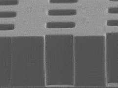
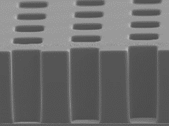
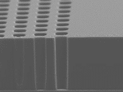
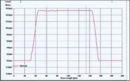
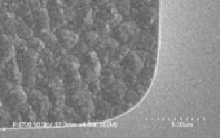
Resist Profile
| S/H 30μm | S/H 20μm | S/H 10μm | |
|---|---|---|---|
| Resist Thickness 65μm |
 |
 |
 |
PMER P-CS Series
This series of resists can be used for precious metal plating processes such as gold and palladium, and has high resistance to metal plating solutions.
Features
- Fine gold plating
- Positive tone type
- Suitable film thickness range = 10~20μm
Photolithography Conditions
Substrate
Au
Film Thickness
20μm
Gold Plating Conditions
Pretreatment
O2 plasma ashing
0.15torr, 300W, 40℃, 60sec
Plating
Cyanide gold plating solution
Resist Stripping
TOK's resist stripper ST-120
Pd Plating Conditions
Plating Solution Type
Pd plating solution pH = 7.5
Plating Conditions
1.5ASD 50℃, 48.6min
Pd Plating Thickness
18µm
Resist Stripping
ST-120, 45℃, 10min
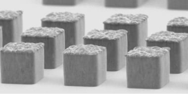
Gold Plating Shape After Resist Removal
| L/S=20/20μm | 20μm Square Pillar Plating Shape |
|---|---|
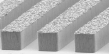 |
 |
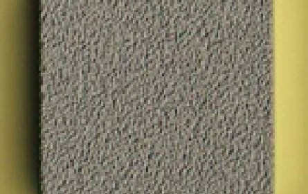
Palladium Plating Shape
Please Feel Free to Contact Us for More Information
For any questions or concerns,
Send an Inquiry Through the Web
Contact Us/Download Information
Please contact us if you have any requests or problems.
You can also access information related to each product.