Tokyo Ohka Kogyo Product Site
Semiconductors
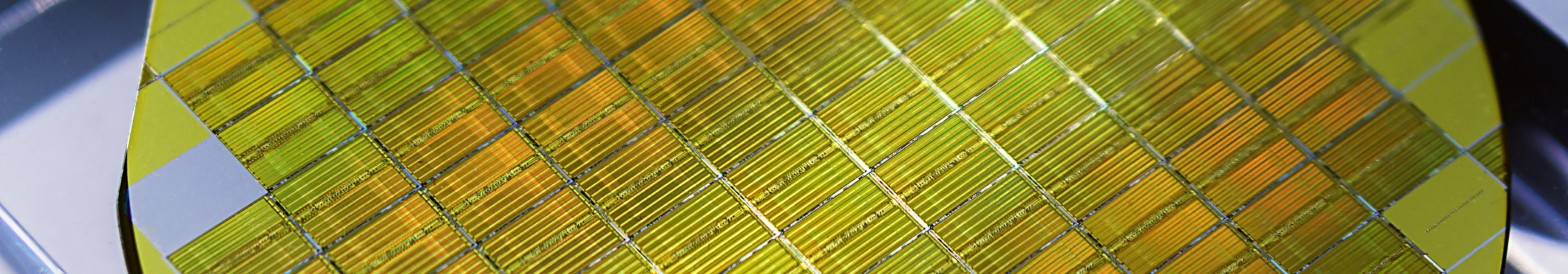
Photoresists provided by Tokyo Ohka Kogyo are indispensable for semiconductor manufacturing. The company also provides high purity chemicals and equipment for the photolithography process, which uses light to achieve fine processing. The following will provide an overview of the semiconductor manufacturing process and the products used.

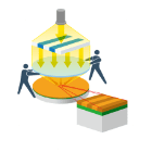


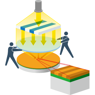
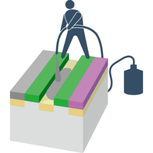
Process1 Photoresist Coating
Photoresist attributes its name due to its photosensitive properties,
specifically that it is a material that changes in response to light. The first step in the semiconductor interconnect manufacturing process is to apply photoresist to the silicon wafer (thin, disc-shaped). We offer a wide range of photoresist materials as well as coating equipment to meet a variety of requirements and conditions.

Related Products

Process2 Exposure
The photomask (blueprint) is transferred to the photoresist just as a photograph is burned onto photographic paper.
The photoresist used in the photolithography process can be either negative, where the exposed areas do not dissolve in the developing solution and remain as a pattern, or positive, where the exposed areas dissolve in the developing solution and the unexposed areas remain as a pattern. There are also various wavelengths of light, and we handle photoresists that are compatible with all wavelengths, from g-line to EUV.
Related Products


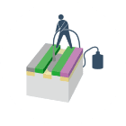
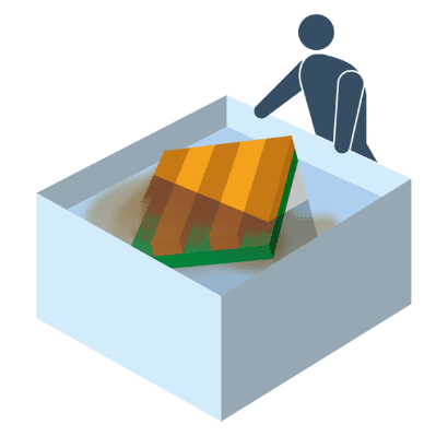
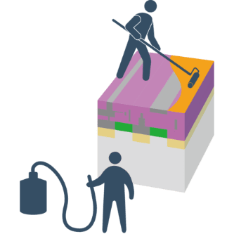
Process3 Developing
The blueprint pattern transferred to the photoresist through exposure is formed in a fashion similar to developing a photograph.
In order to form the pattern, the unnecessary parts of the resist are dissolved and removed by dipping in a special developer that is compatible with various types of photoresists. We offer a variety of developer solutions for different types of resists.
Related Products

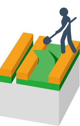
Process4 Etching
The photoresist pattern formed after developing is used as a protective film, and areas without photoresist are etched. There are two types of etching: dry etching and wet etching.
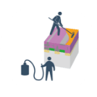
Process5 Photoresist Removal
Photoresist that is no longer needed is removed. Using the appropriate stripper for each type of photoresist, the photoresist can be removed swiftly. We provide high purity cleaning solutions, stripping solutions, and thinners.

Related Products

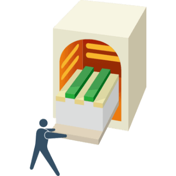
Process6 Formation of Semiconductor Region
After coating the wafer with a material to diffuse impurities, the wafer is baked at high temperatures to form the semiconductor region. We also provide diffusion materials.
Related Products
Process7 Formation of Insulating Film and Wiring
Aluminum or copper is used to form the wiring. We provide materials to form interlayer insulating films.
Related Products

Process8 Formation of Integrated Circuits
These processes are repeated to form the integrated circuits and complete the semiconductor devices on the wafer.
Related Products

Related Information
Contact Us/Download Information
Please contact us if you have any requests or problems.
You can also access information related to each product.