Tokyo Ohka Kogyo Product Site
Semiconductor Packaging
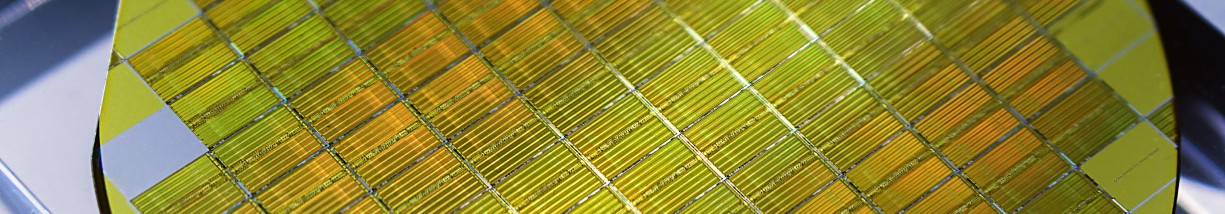
In addition to increasing the performance of electronic devices such as smartphones with semiconductor devices and electronic components, efforts to make them lighter, thinner, and smaller are progressing faster than imaginable. Packaging technology plays an extremely important role in realizing these lightweight, thin, small profile, power saving, and high-speed communication characteristics.
Tokyo Ohka Kogyo (TOK) develops and commercializes photoresists that are optimal for various packaging processes, even the most advanced. As for packaging photoresists, the company offers photoresists for a wide range of production technologies, including wafer-level CSP, SiP, redistribution layer (RDL), TAB, and COF.

Semiconductor Packaging (Back-End Processing)
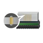
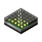
Wafer Cutting
The wafer is cut to the size of the semiconductor chip.
Dicing Process Surface Protection Film
Protects the surface of the wafer during the cutting process. The protective film is water-soluble and can be removed by rinsing.

Related Products

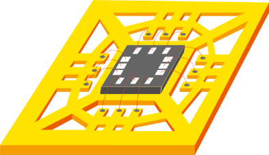
Wire Bonding
Wire bonding is a packaging technique in which a thin metal wire is connected to the metal lead of a leadframe and energized.
Resist for plating
A photoresist for the plating of precious metals such as gold and palladium for LCD drivers.
Related Products

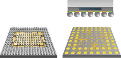
Fan-Out Package
Bumping is the process of placing protruding terminals on the substrate.
We provide photoresists for bump formation, high purity cleaning solutions, thinners, and developers.
RDL/Rerouting Formation
Photoresist for RDL formation of wafer-level packages, fan-out packages, interposers, etc.
Related Products

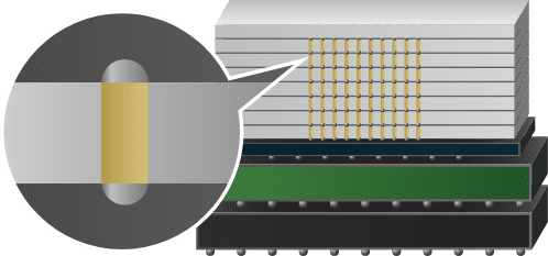
TSV
TSV is a technology where semiconductor chips are stacked in thin pieces and through-hole electrodes are used to connect the chips to each other.
We provide photoresists for TSV, photoresists for rewiring plating, adhesives, and thinner for adhesives.
TSV Mounting
Resist for plating microbumps and through-copper electrodes for 2.5D and 3D semiconductor packaging, and high heat-resistant thick-film resist for Si deep etching.
Related Products


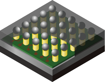
Cu Pillar Wafer Level CSP
To protect semiconductor devices from impact and contamination, special resin is used to fix semiconductor chips.
Solder bumps for flip chip BGA packages, thick film plating resist with excellent resistance to plating solution for the formation of copper pillar electrodes.
Related Products

Related Information
Contact Us/Download Information
Please contact us if you have any requests or problems.
You can also access information related to each product.