Tokyo Ohka Kogyo Product Site
Sensors
Semiconductor and MEMS sensors are not only based on silicon substrates, but also on glass substrates and organic materials, where microfabrication techniques are used to create unique shapes and structures in addition to electronic circuits. Tokyo Ohka Kogyo develops material that are most suitable for such special processes.

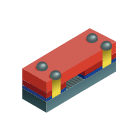


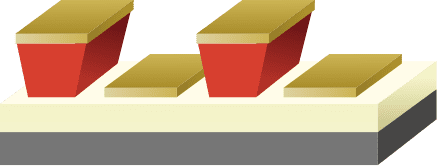
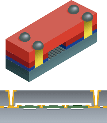
Lift-Off Process
From the reverse tapered resist pattern, the desired metal and wiring layers can be formed on the substrate through metal deposition or metal sputtering without the need for etching.
Related Products

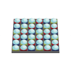
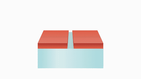
Cavity Formation
Thick film interconnects can be used to create hollow cavity structures.
Related Products


Transparent Layer Formation
High transmittance films can be formed through photolithography technology. They can be processed post-patterning such as through baking and etching.
Related Products


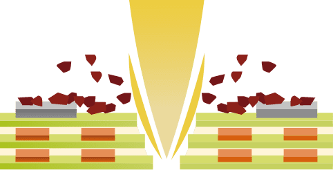
Stain Resistance Process
These products are used to prevent debris from being deposited during blade∕laser dicing. The same materials can also be used as a mask material during plasma dicing.
Related Products

Glass Processing

Related Information
Contact Us/Download Information
Please contact us if you have any requests or problems.
You can also access information related to each product.