Tokyo Ohka Kogyo Product Site
Technical Information

Tokyo Ohka Kogyo is focusing on creating demand in new fields based on the development capabilities, responsiveness, and high value-added products we have cultivated in the semiconductor photoresist business.
We regularly update our technical information. Please feel free to contact us if you would like to know more about our products and services.
We hope that you will find our latest technical information useful for development in a variety of fields.
Technology Information List
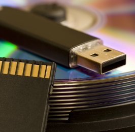
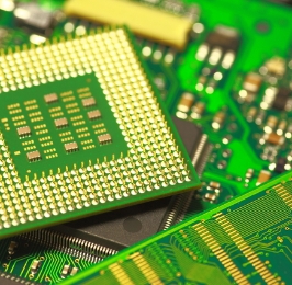
Semiconductors

What is Double Patterning?
This section discusses "double patterning," used in the manufacture of nm-class processes when ArF immersion lithography system and other methods cannot resolve the image.
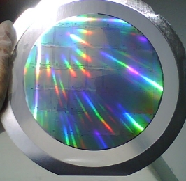
Semiconductors

Development of Low Defect Positive Photoresist for Immersion ArF
This section discusses "low defect positive photoresists for immersion ArF," materials for processing semiconductors using ArF immersion lithography equipment.
Semiconductors
Development of Thick Film Positive Photoresist for KrF 3D-NAND
Chips produced using this product are used in smartphones, now beloved worldwide.
Semiconductors
Development of Cleaning Solutions for Advanced Semiconductor Processes
We are also involved in the design and development of cleaning solutions with new functions to remove unclassified debris from semiconductors.
Semiconductors

I-Line Photoresists That Contribute to Power Semiconductor Production
Photoresists for i-line were introduced in the late 1980s. Even today, while KrF photoresists have replaced it in feature miniaturization, i-line photoresists continue to play an active role.
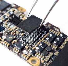
Semiconductors
Semiconductor Packaging
TMMR & TMMF Series (Development of Photosensitive Insulating Materials)
This section discusses "SAW filters," which contribute to the downsizing, high performance, and multi-functionality of cell phones and other devices by taking advantage of its low profile and lightweight characteristics.
Semiconductor Packaging
TLDP Development
This section discusses "TLDP," used in the dicing process to cut semiconductor chips into chips for packaging.
Semiconductor Packaging
Development of PMER P-CX and P-CZ Series Thick Film Resists for High Speed Plating
This section introduces technology behind our products that are used in the latest semiconductor packaging industry.
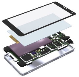
Semiconductor Packaging
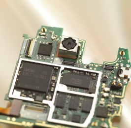
Development of High Speed Cu Pillar Plating Materials for WL-CSP
Our photoresists for packaging are used in the semiconductor packaging technology for smart phones. Included here is an explanation of this packaging technology and the features of our products.
Semiconductor Packaging

Development of Cu RDL (Redistribution Layer) for FO (Fan Out) Packages
We will introduce our technology for fan out packages that can be used for multi-chip applications without being limited by chip size.
Semiconductor Packaging
Sensors
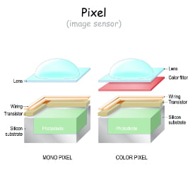
Development of High Heat Resistance, High Transparency Microlens Resists Using Novel Polymer
Image sensors are widely used in medical fields and for car cameras. Our "microlens resists" are used in these sensors.
Sensors
Contact Us/Download Information
Please contact us if you have any requests or problems.
You can also access information related to each product.