Tokyo Ohka Kogyo Product Site
Product & Business Overview
Exploring New Fields Based on Technology Cultivated in Semiconductors
Since its founding in 1940, Tokyo Ohka Kogyo has been developing its business in the field of fine chemicals by pursuing cutting-edge technologies as an R&D-oriented company and expanding its technologies from high purity chemicals to high-performance photoresists for photosensitive materials.
While we have continued to create value in niche, cutting-edge fields, we are confident that our products and technologies will contribute to an even wider range of fields as we move into the future with new innovations in AI, IoT, and 5G.
Based on our flexible development capabilities cultivated in the semiconductor industry, we will continue to refine our products and technologies and boldly take on new development themes. Please take a look at our core technologies detailed below and do not hesitate to contact us regarding applying them, regardless of field.

Did You Know?
There Are 12 Core Technologies at Tokyo Ohka Kogyo
This year TOK celebrates its 80th anniversary.
Though long time customers may see TOK mainly as a provider of photoresists, our product lineup and technical expertise ranges well beyond these materials.
Please witness the “seeds of technology” from our 12 core technologies that could be utilized at your company.
Microfabrication Technology
At the core of Tokyo Ohka Kogyo technological prowess is the world’s highest standard of microprocessing.
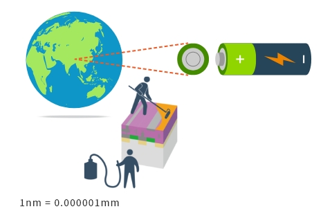
Current demand for microfabrication technology using photolithography requires processing accuracy at the nanometer (nm) scale. We have developed a range of Extreme Ultraviolet (EUV) photoresists for the world’s smallest circuit widths at 7nm. We have also accumulated the world’s highest level of development and manufacture in the following technological fields.
High Purification Technology (ppq Level)
We provide the world’s purest chemicals (cleaning solutions, thinners, developers, etc.) for microfabrication technology. In doing so, we contribute to the increasing yield rate for mass production of devices. Our high purification technology has evolved with the times, with impurities in our products starting at less than 1ppm (parts per million), and now reaching ppq (parts per quadrillion) for some products.
We demonstrate our strengths in tackling challenges such as through development of high quality grade solutions and performance control of particle sizes in response to customers’ processes.

Detection Sensitivity of Metal
Impurities in High Purity Chemicals
Below 10ppt or 1/100,000,000,000
Full Wavelength Compatibility
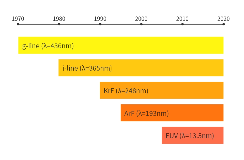
Alongside development of semiconductors, the resolution of lithography tools used in photolithography has been gradually improving, and light sources have changed from g-line (436nm) to i-line (365nm), KrF excimer laser (248nm), ArF excimer laser (193nm), and now EUV (13.5nm), the next generation in lithography technology, in order to provide ever shorter wavelengths necessary. We deal with photoresists for various light sources to cover all wavelengths, which allows customers to choose the best product according to functional requirements.
Customizability
Semiconductor manufacturing processes vary depending on the customer and the type of product, so photoresists and chemicals used as materials must be tailored quickly and accurately to the requirements of each customer.

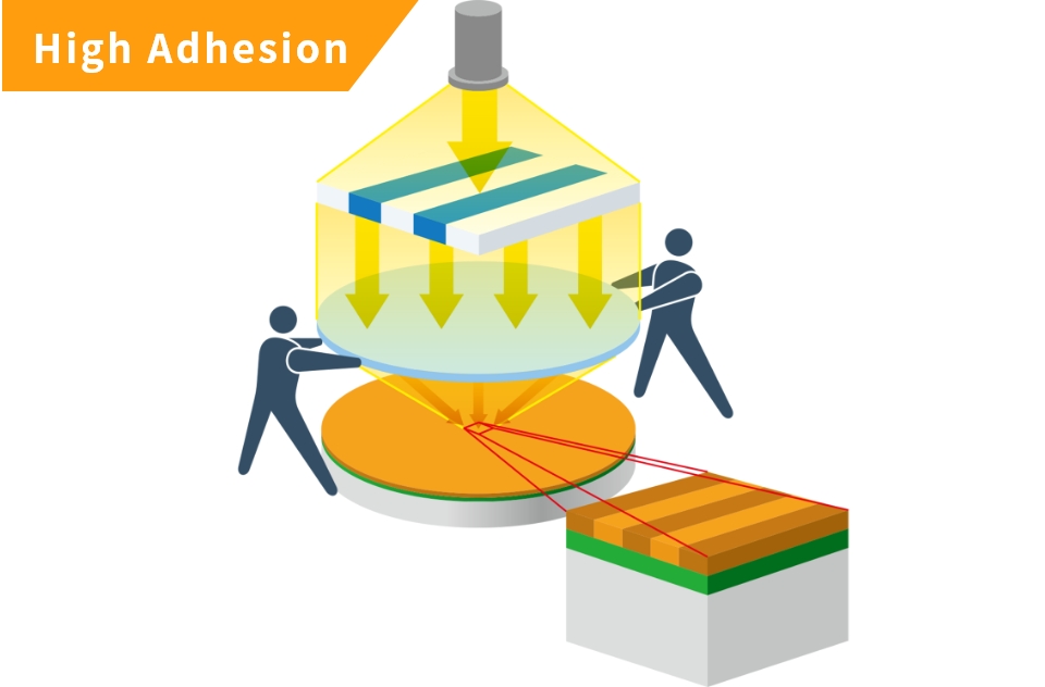
High Adhesion
In the process of photolithography, it is important to achieve good adhesion between the semiconductor substrate and the photoresist.
In particular, the most advanced packaging processes and MEMS manufacturing processes, which support weight reduction, thinness, and low profile of high-performance mobile devices and electronic components, require materials with superior adhesion.
Our company has developed a range of photoresists to support the miniaturization and performance of such electronic components, including plating photoresists for high density packaging, MEMS manufacturing processes and photosensitive permanent film photoresists.
Photosensitive Material Know-How and Application
We are developing high value-added products that can be used to solve the problems in the new era by utilizing our accumulated expertise in photosensitive materials.
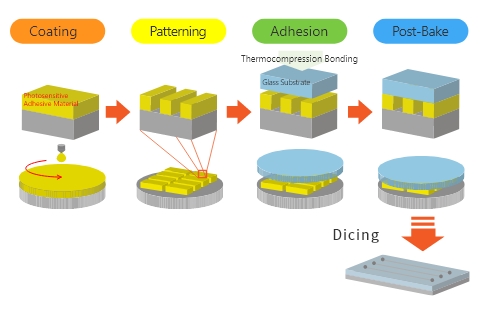
Photosensitive permanent film photoresists can be used to form MEMS structures, greatly simplifying the process compared to conventional sacrificial film methods. In addition, we have a range of photosensitive adhesive materials that enable photolithographic patterning and substrate bonding in a single material. Furthermore, we are working on the development of nanoimprint materials, a new business field based on photosensitive material technology.
Shape Control
It is possible to form a laminating film that can control not only the rectangular shape from the material design but also the tapered shape and reverse-tapered shape. We also have products that can be molded into specific shapes (hemispherical, etc.) by undergoing additional processes such as baking after patterning.

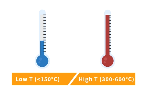
Addressing Low T (<150°C) and High T (300-600°C)
We are developing resists for film substrates that can be permanently cured at low temperatures, as well as products that can be used at temperatures up to 600°C using Si-containing resins.
Coloration (Transparent, Refractive Index Adjustment)
We offer several types of transparent film materials with high transmittance in the long wavelength range. Furthermore, we offer materials that alter refractive index.

Stripping and Reworkability
We have developed a lineup of high purity strippers and cleaners that selectively remove only specific target materials (resists, etching residues, metal altered films, etc.) through our original chemical formulation technology and granting new properties using organic and inorganic chemicals. This available lineup can also meet the environmental regulations of each region.

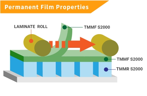
Permanent Film Properties
Permanent films are permanent epoxy resin-based films with high resolution photosensitivity. They have high resolution, high adhesion, and can be used to form fine patterns with high aspect ratios. They are suitable for forming interlayer insulators, hollow structures for flow channel MEMS, and cavity structures for SAW/BAW filter RF devices. Both film type for lamination and liquid type for spin coating are available.
We also offer products with low autofluorescence, which is required for BioMEMS.
Quality Stability (Production Technology)
The chemicals we manufacture are SPC-controlled at the time of production to ensure semiconductor-grade specifications and to avoid differences among lots, thereby ensuring stable quality. This is done using the technology and know-how we have cultivated over many years of production.

Contact Us/Download Information
Please contact us if you have any requests or problems.
You can also access information related to each product.