Tokyo Ohka Kogyo Product Site
Development of Thick Film Positive Photoresist for KrF 3D-NAND

What is 3D-NAND?
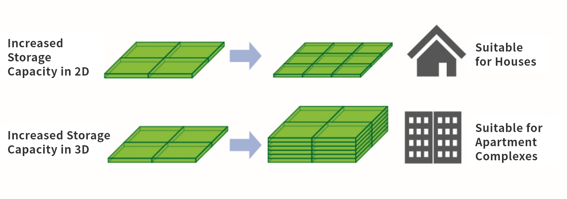
NAND flash memory is found in SD cards, USB flash drives, and smartphones. This is a type of semiconductor that can retain memory even when the power is turned off, is compact and lightweight, is resistant to vibration and shock, and has low power consumption. With the increase in the number of cells, which are the data storage components, the storage capacity also grows, making it possible to store more photos and videos in a smartphone (increased storage capacity). Until now, increasing the number of cells over a given surface area has been the only way to achieve increased capacities (Fig. 1). However, increasing the number of cells also means narrowing the gap between cells, which causes electrical interference between adjacent cells and makes it easier for malfunctioning to occur. Therefore, simply increasing the number of cells on a flat surface area through miniaturization to achieve higher capacity has become extremely difficult. Therefore, "3D-NAND" has emerged as a promising solution for increasing the volume. In contrast to the conventional method of arranging cells on a flat surface (2D), 3D-NAND has a structure in which cells are stacked vertically (3D). By stacking in the vertical direction, it is possible to achieve greater storage capacity than ever before (Fig. 2).
Fig. 1 - Evolution of NAND Flash Memory
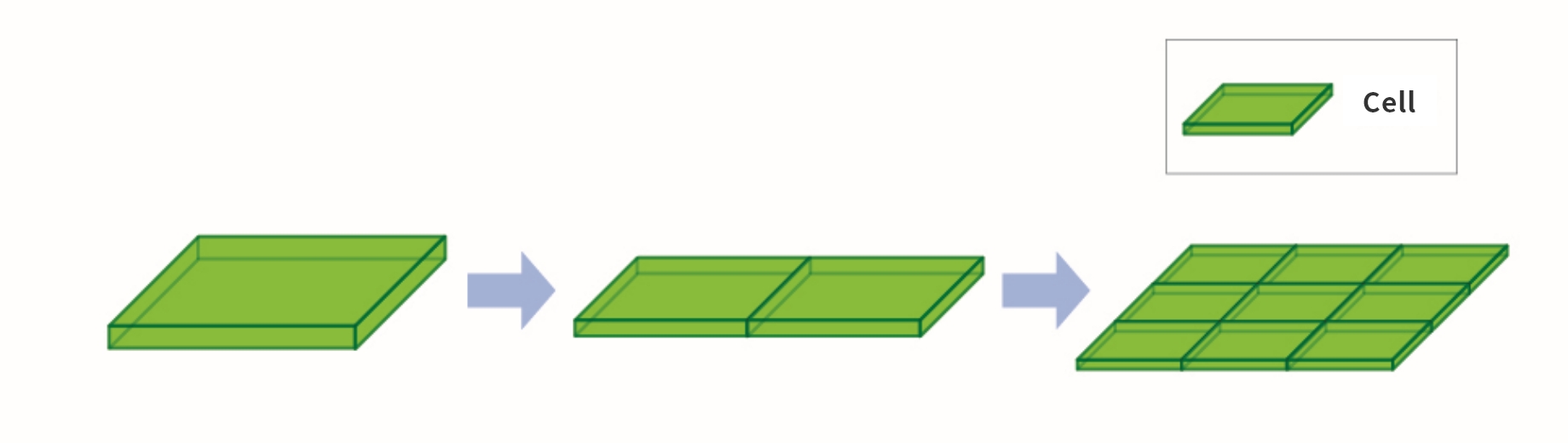
Fig. 2 - Increasing Storage Capacity in 2D and 3D
Product Features
3D-NAND requires processing a staircase structure in order to control the cells in each layer, and a photoresist is used to form this staircase. The resist is not designed for the conventional resolution, but rather for the 3D-NAND pyramid structure formation (Fig. 3). In order to process multiple staircases in the same manner quickly and accurately, it is difficult to simply increase the thickness of the conventional resist (film thickening), and for this purpose it is important to consider the physical properties of the resist in addition to the lithographic properties. This is where our pool of knowledge and ideas can help to satisfy both of these factors.
Fig. 3 - Basic Structural Image of 3D-NAND
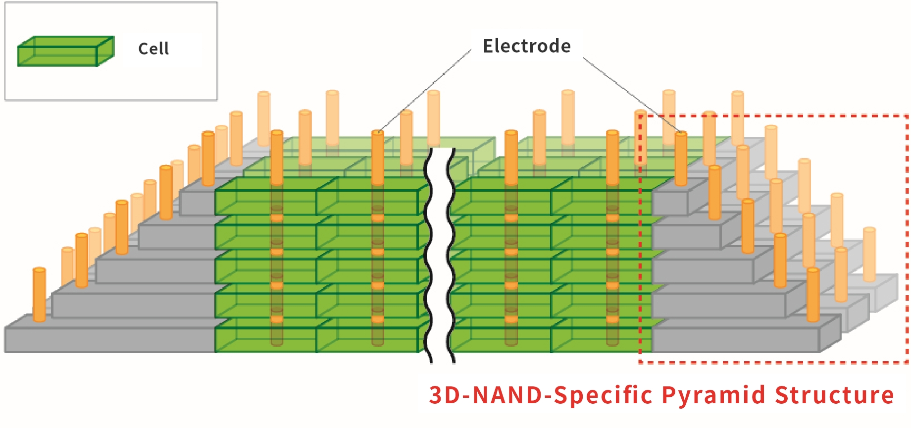
It has a pyramid structure with a storage section and a staircase section to form electrodes that conduct electricity to each layer.
Contact Us/Download Information
Please contact us if you have any requests or problems.
You can also access information related to each product.