Tokyo Ohka Kogyo Product Site
Development of Cu RDL (Redistribution Layer) for FO (Fan Out) Packages

What is Fan Out Packaging?
Semiconductor packaging technology not only protects IC chips from external impact, but also contributes to the creation of semiconductor products for a wide variety of uses by arranging chips and various types of wiring in different ways. Unlike the conventional fan in package, the fan out package is not limited by the size of the chip, and has the advantage of multi-chip placement, which is expected to improve the performance in a manner unachievable with conventional packaging. As such, fan out packages are used in high performance smartphones.
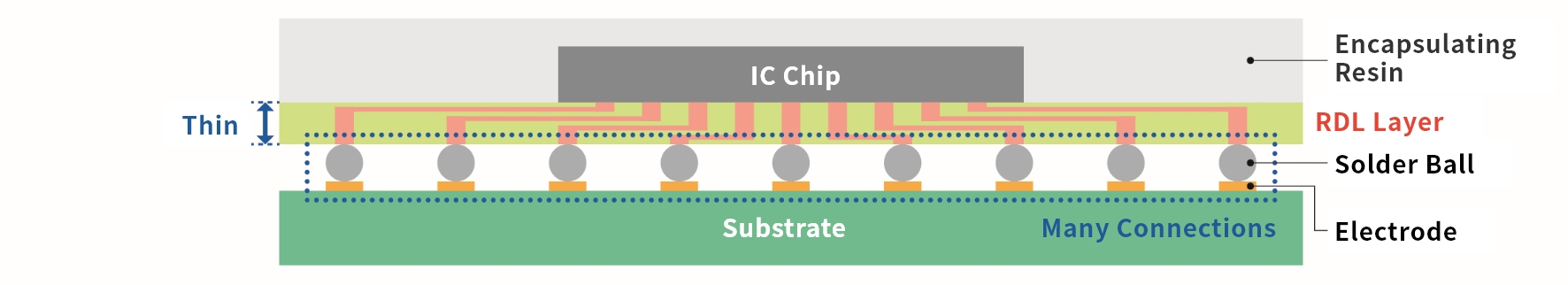
The key to the fan out package is the wiring layer called redistribution layer (RDL), which is used to input and output information to and from the IC chip, respectively (Fig. 1). This RDL is formed by making a pattern mold with photoresist and performing electrolytic copper plating on it. In the past, there were no resists in the industry that were specifically designed for this RDL process, and resists for forming bumps were used in tandem. However, as time went on, there was a demand for resists specialized for high resolution RDL to support higher performance application processors.
Our company offers a wide range of products to meet the needs of various customers in this field.
Fig. 1 - FO Packaging
Contact Us/Download Information
Please contact us if you have any requests or problems.
You can also access information related to each product.