Tokyo Ohka Kogyo Product Site
Development of High Speed Cu Pillar Plating Materials for WL-CSP

What is WL-CSP (Wafer-Level Chip Scale Packaging)?
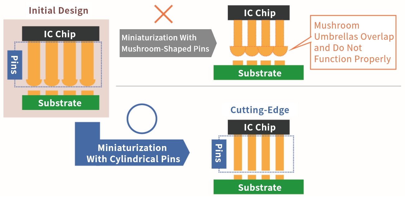
In order to improve the performance of smartphones, it is important to be able to mount more IC chips. However, the limited surface area means that the IC chip must also be compact, and the evolution of packaging technology has played a major role in the miniaturization of semiconductors.
In order to reduce the size of an IC chip, there is a packaging technology called flip chip that has compact pins. When this technology was first developed, mushroom shaped pins were used, but with further improvements in performance of smartphones, a technology called WLCSP (Wafer-Level Chip Scale Packaging) was developed, and cylindrical pins were used. This technology is utilized in the most advanced smartphones.
Transition Chart of Packaging Technology
TOK Product Features
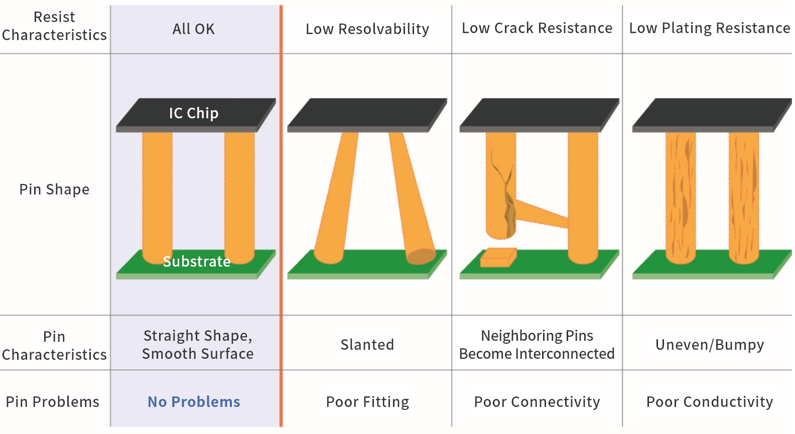
In order to support WL-CSP technology, which is now used in the manufacture of advanced IC chips, we provide resists that enable high speed formation of Cu pillars. This resist is characterized by its ability to simultaneously satisfy three rather contradictory characteristics: resolution for inserting a specific number of pins on a limited surface area, crack resistance to prevent poor bonding with the substrate, and plating solution resistance to prevent the pins from becoming distorted which would impede the flow of electricity. Satisfying these three characteristics at the same time is very difficult, similar to attempting to uniting three extremely capable but selfish employees into a single team while making the most of their individual abilities. This product was developed to overcome such an extremely high hurdle. The chips produced with this product are used in smartphones, which are now globally beloved.
Contact Us/Download Information
Please contact us if you have any requests or problems.
You can also access information related to each product.