Tokyo Ohka Kogyo Product Site
TLDP Development

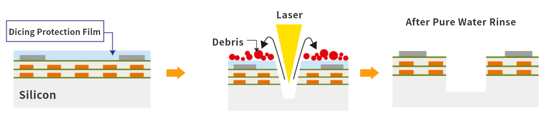
What is Dicing Protection Film?
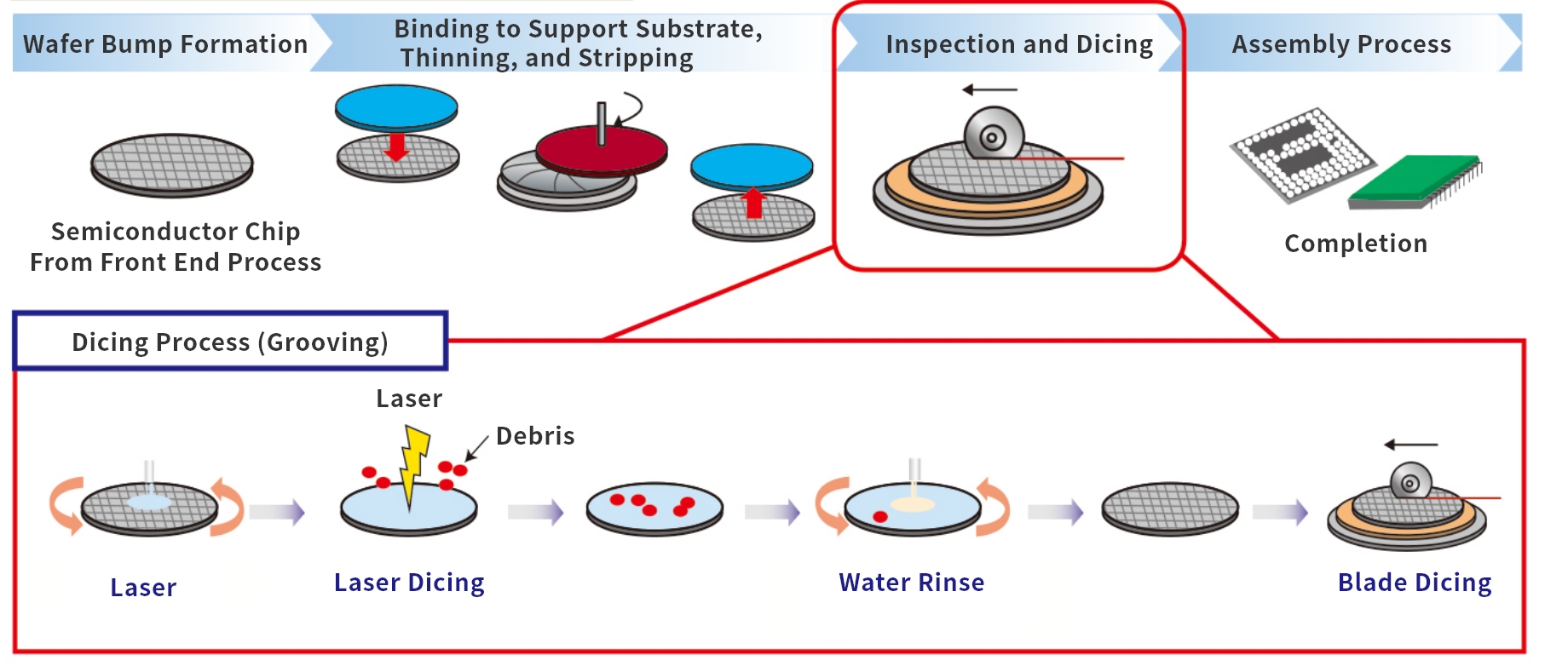
The process of manufacturing semiconductor chips is divided into three major parts: the design/masking process for forming masks to manufacture chips, the front end process for forming integrated circuits on wafers, and the back end process for sealing the semiconductor chip into various packages for commercialization.
The dicing protection film is used in the dicing process where the wafer is cut into chips using a specialized cutter (dicing saw) in order to package the semiconductor chips.
TLDP in the text are pending or registered trademarks of TOK.
The Assembly, Packaging and Inspection Process (Back End)
What is Dicing Protection Film?
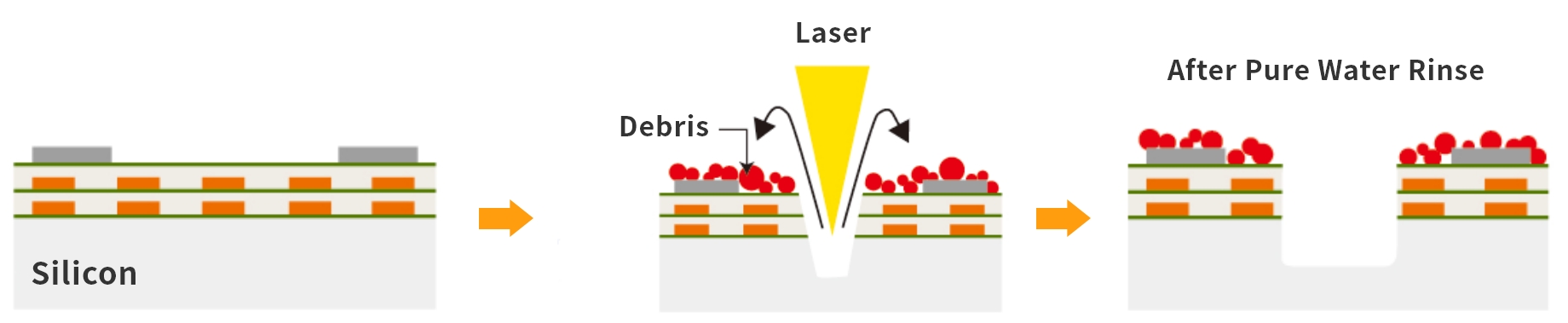
The dicing protection film is used to protect the substrate to prevent adhesion of debris during laser dicing. During dicing, oxides and dissolved metal particles are generated on the surface of the wafer, which are difficult to remove completely during the cleaning process.
The dicing protection film is made from a water-soluble resin and is applied to the processing surface in advance to prevent debris from sticking to the substrate, and allowing complete removal of debris during the water rinsing process afterward.
Comparison With and Without Dicing Protection Film
Without Dicing Protection Film
With Dicing Protection Film
Contact Us/Download Information
Please contact us if you have any requests or problems.
You can also access information related to each product.