Tokyo Ohka Kogyo Product Site
Development of Cleaning Solutions for Advanced Semiconductor Processes
The Importance of Cleaning Solutions
In order to manufacture semiconductors, the wafer substrate must be kept clean at all times. However, in each of the hundreds of semiconductor manufacturing processes, small particles are generated and stick to the wafer. This debris is not easily removed, and if it remains can cause semiconductor defects (e.g. electrical signal interference). In order to reduce the failure rate, such debris must be thoroughly removed (cleaned). Chemicals used to remove this dust are the cleaning solutions (Fig. 1).
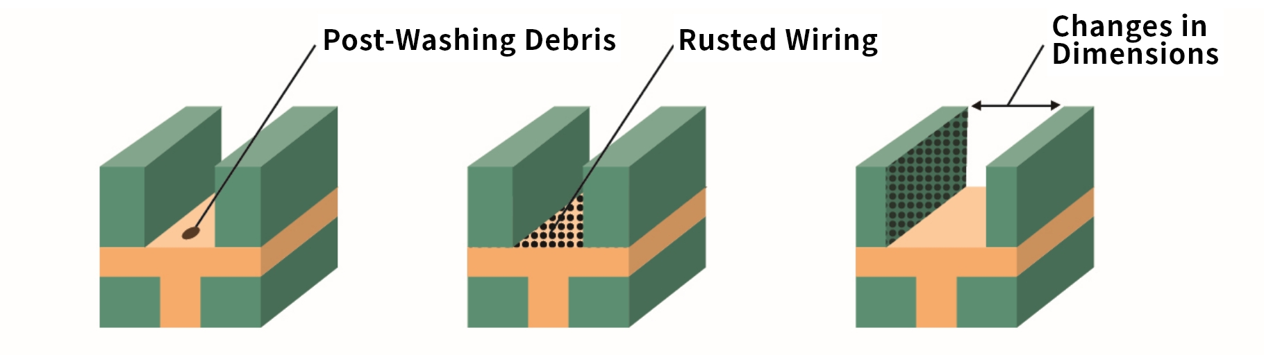
In addition to the removal of debris, unintended chemical reactions between the cleaning solution and the material may cause damage to the material, such as rusting of wiring or changes in shape (Fig. 2). Since this damage can cause various defects, it is not sufficient to enhance the cleaning solution's ability to remove particles alone. The cleaning solution must be able to fulfill two completely different functions of both removing debris and protecting the semiconductor.
Fig. 1 - The Significance of the Cleaning Process
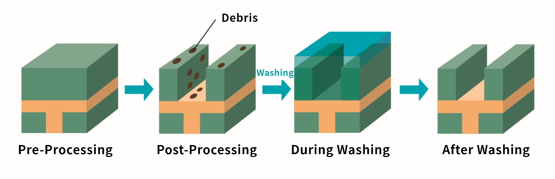
Fig. 2 - Examples of Poor Cleaning and Damage
In order to improve the performance of semiconductors, changes are introduced in the materials (e.g. aluminum → copper) and structures (e.g. 2D → 3D). As a result, the nature of the generated debris also changes drastically, and TOK is designing and developing cleaning solutions with new capabilities to deal with yet unclassified debris.
*The following table shows the types of waste that can be removed through the process (a wide variety of debris exists, including etching residue and resist residue).
Contact Us/Download Information
Please contact us if you have any requests or problems.
You can also access information related to each product.