Tokyo Ohka Kogyo Product Site
What is Double Patterning?

What is Double Patterning?
With the aim of improving the productivity and functionality of semiconductors, the line widths of circuits inside semiconductors have been decreasing in size with each generation.
Particularly in semiconductors such as CPUs and memory used in PCs and smartphones, miniaturization is being carried out using a variety of methods since miniaturization contributes greatly to high performance and low surface area. In the past, miniaturization was achieved by increasing the length of the lens and the number of lens apertures in the exposure tool, and this is exactly how miniaturization progressed until the ArF excimer laser (193nm). However, it was expected that it would take a long time to solve the technical issues of equipment and material development for further shortening the wavelength from ArF excimer laser, and so the double patterning technology was developed to achieve miniaturization using existing exposure systems. Various processes using double patterning with ArF immersion lithography for miniaturization were investigated, including methods with multiple exposures as well as a method of reducing the size of the pattern by half from the deposition technology based on the formed pattern.
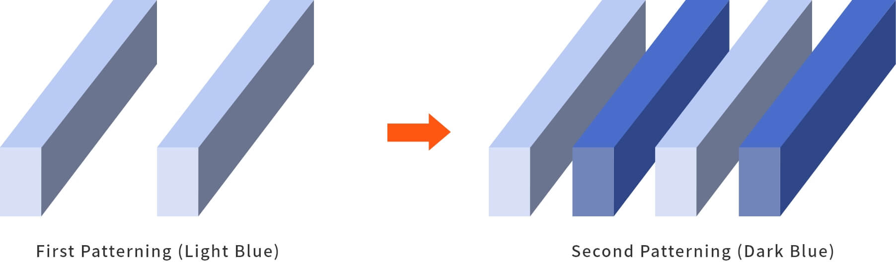
In the multiple exposure technique (multiple masks may be used), the process of photoresist
deposition=>exposure=>development (patterning)=>etching (transfer to substrate) is repeated in different positions to reduce the line width (line repetition width). In this method, there is freedom of pattern design, but positional displacement accuracy is very important.
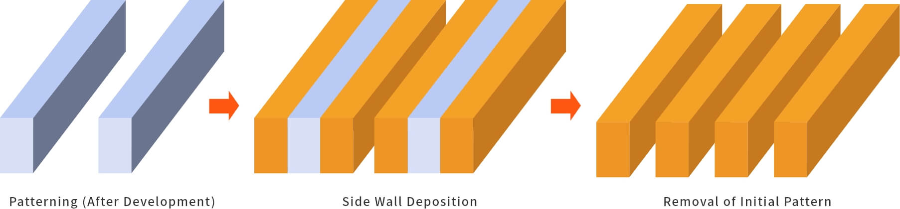
A method of halving the pattern size from a deposition technique (self-aligning double patterning) involves forming a half size pattern on the side walls of a resist or transferred pattern on a substrate using a deposition technique called CVD to achieve the desired size. In this case, the positional accuracy is dependent on the initial pattern size and can be controlled with high accuracy, but there is no freedom in pattern design. This technique can also be repeated to reduce the size of the pattern to a quarter.
Currently, the two double patterning techniques described above are the mainstream, and the double patterning using ArF immersion lithography forms a line width of 30nm or less to create the circuitry in the semiconductor. TOK is continuing to develop new materials to meet such technical demands.
Terminology
| 1) 1nm | One billionth of a meter |
|---|---|
| 2) ArF | An abbreviation for Argon Fluoride, the light source (193nm) used in the most advanced fabrication parts in the world today |
| 3) Etching | The process of processing the surface of an object by using a chemical or other corrosive effect |
| 4) Freezing | A material that protects the initially formed resist pattern from dissolving in the solvent of the second coat of resist |
Contact Us/Download Information
Please contact us if you have any requests or problems.
You can also access information related to each product.