Tokyo Ohka Kogyo Product Site
Adhesives

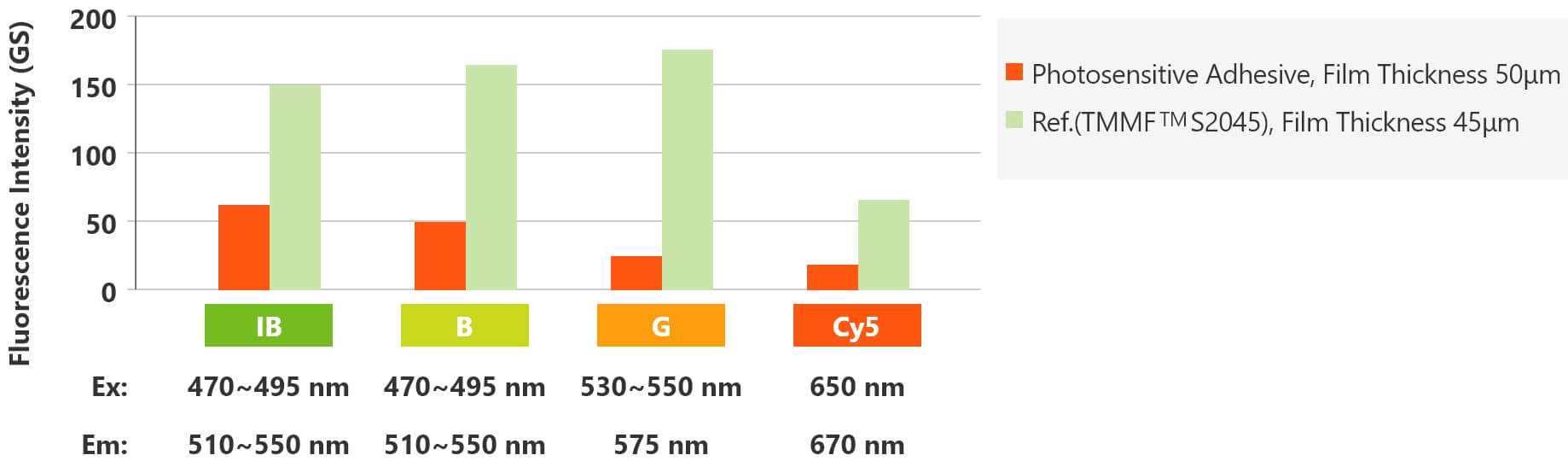
Fine patterning is possible by photolithography process. These photosensitive adhesives are suitable for Si to Si, Si to glass, and glass to glass bonding of semiconductor devices, MEMS sensors, semiconductor substrates, and support plates by selectively forming a fine patterned adhesive layer. It has low autofluorescence and low cytotoxicity, which makes it suitable for BioMEMS.
Photosensitive adhesives with high transmittance (99.9%@400nm, n=1.52@550nm) are also available.
Photosensitive Film Type TMMF NA1000 (Liquid Type TMMR NA1000PM)
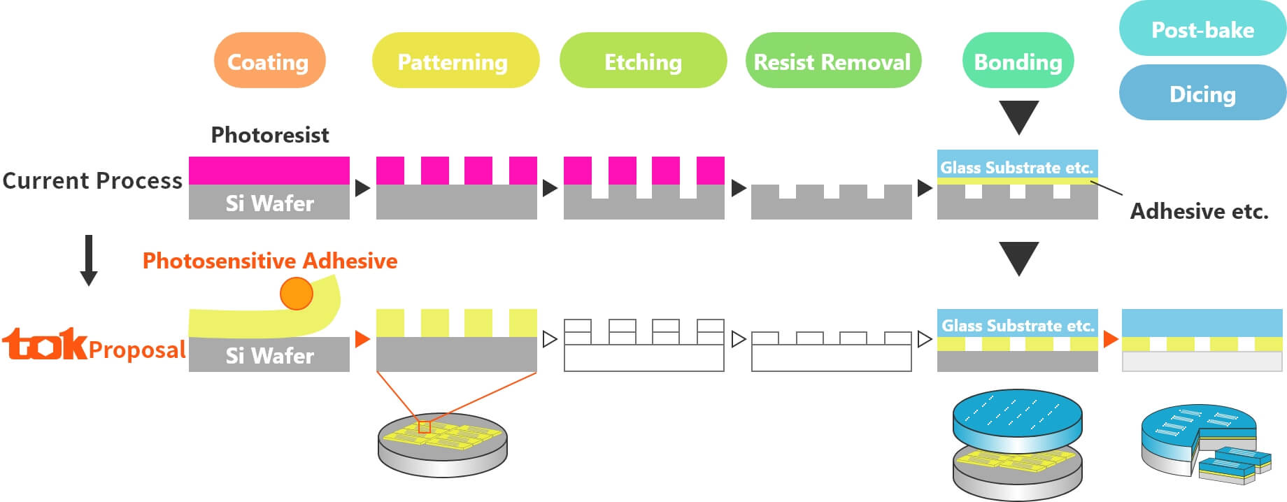
Structure Formation and Substrate Bonding Can Be Done With a Single Material
- Negative type dry film resist (solvent development type)
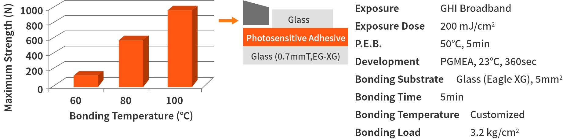
- Suitable for low temperature bonding
- Low auto-fluorescence, extremely low cytotoxicity (ISO-10993-5 compliance)
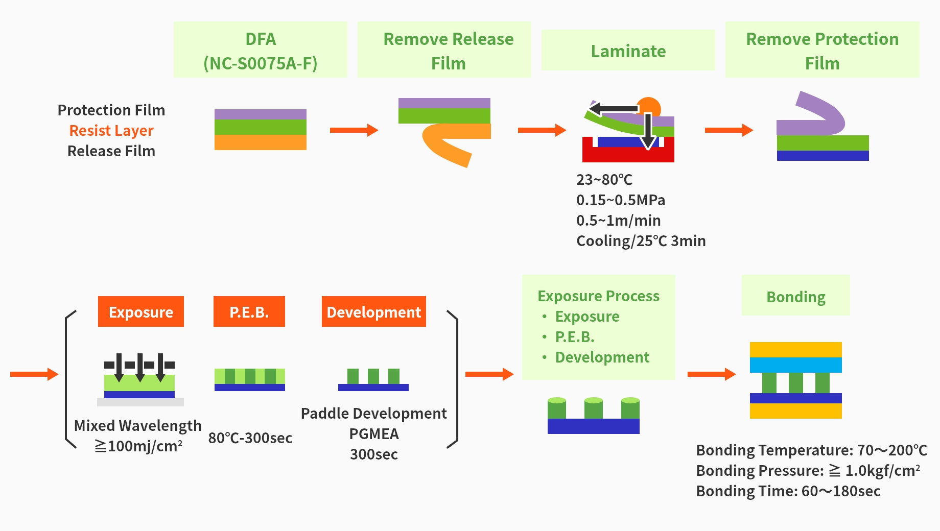
Film Type Process Flow
Applications: Semiconductor chip to chip bonding, semiconductor chip to substrate bonding. Other applications include printer heads, LEDs, TSV bonding, semiconductor and sensor module manufacturing.
- Low Temperature Curing (200℃)
- PGMEA Development
- Good Adhesion
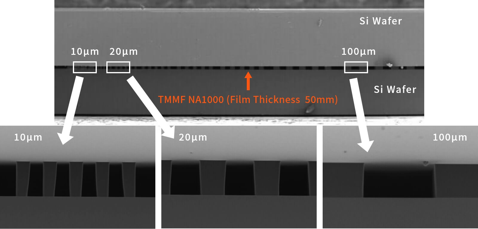
- Suitable film thickness range (5~60μm)
- High heat resistance (up to 280℃)
- Chemical resistance
Bonding Strength
Auto-Fluorescence
We offer two types of products: the film type TMMF NA100 for lamination and the liquid type TMMR NA100 for spin application.
TAMFC, TMMF, and TMMR in the text are pending or registered trademarks of TOK.
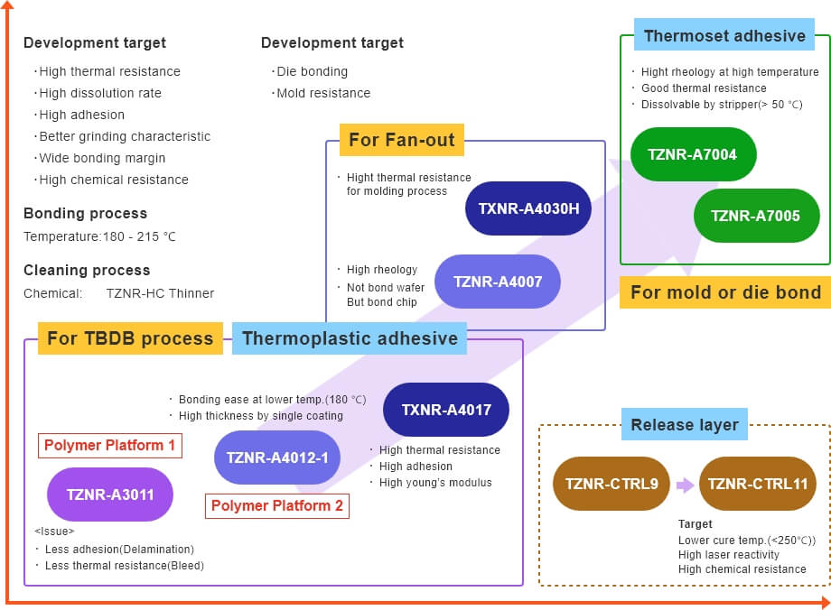
Temporary Adhesive for TBDB
Tokyo Ohka Kogyo has developed a unique wafer handling system (ZeroNewton) for three-dimensional packaging technology (3D as well as 2.5D), in which wafers are thinned and stacked as a solution for advanced packaging, and provides temporary adhesives for this process.
We provide temporary adhesives for fan-out wafer level processes (FO WLP) and also panel level processes (FO PLP).
Three-dimensional Mounting Process Wafer Level TSV
Three-dimensional mounting technology is one in which thinned semiconductor wafers with electronic circuits are stacked three-dimensionally. Since through-silicon vias electrodes are used to conduct current between the layers, many advantages can be attained, such as miniaturization, higher density, and power saving for semiconductors, as well as faster signal transmission and processing speeds.
For this stacking process, Tokyo Ohka Kogyo has developed a process for attaching and separating semiconductor wafers to supporting glass layer(s). This wafer handling system is state of the art processing technology that enables significant efficiency improvements in the three-dimensional mounting process and supports further enhancement in semiconductor performance.
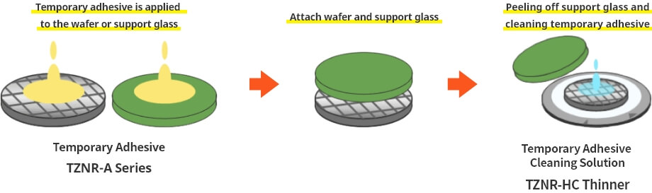
Temporary adhesive is applied to either the wafer or support glass, and the support glass and wafer are attached together.
After backside processing (thinning, device fabrication), the support glass is peeled off and cleaned.
Three-dimensional Mounting Process Wafer level Fan-out
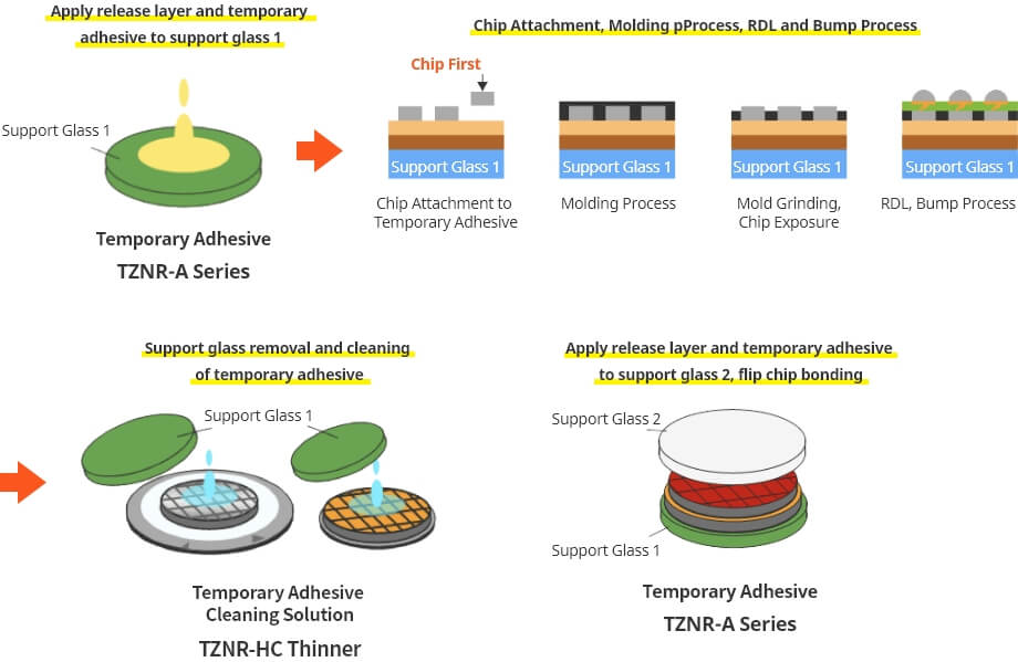
Temporary adhesive is applied to the support glass, which has release layer applied.
After chip attachment, molding process, RDL and bump process, support glass 1 is peeled off and cleaned.
As an option, support glass 2 can be attached to the substrate after RDL and bump, and the same process can be performed on the support glass 1 side.
Development History of Temporary Adhesives
ZeroNewton and TZNR in the text are pending or registered trademarks of TOK.
Temporary Adhesive Data
| Process | Target Process | TBDB | Fan-out | |||
|---|---|---|---|---|---|---|
| Measurements | A4012-1 | A4017 | A4035 | A4007 | A4030H | |
| Coating | Standard (μm) (Viscosity) |
35~100 (10000cP) |
35~100 (10000cP) |
35~100 (10000cP) |
5~10 (300cP) |
5~10 (300cP) |
| Die Bonding @ Low Temperature |
Young's Modulus [GPa] (measured by Fisher HM) |
0.15 | 0.22 | 0.53 | 0.04 | 0.43 |
| Modulus E*at 100℃ [KPa] (1Hz, Rheology) |
1200 | 4680 | 156000 | 9700 | 187000 | |
| Heat Resistance | △5% Weight Loss Temperature (TGA) [℃] | > 350 | > 350 | > 350 | > 350 | > 350 |
| Degassing (TDS) | Good | Good | Good | Good | Good | |
| Modulus E* or G*at 180℃ [KPa] (1Hz, Rheology) |
68(G) | 138 | 725 | 321(G) | 7000 | |
| Modulus E* or G*at 200℃ [KPa] (1Hz, Rheology) |
26(G) | 36(G) | 55(G) | 312(G) | 1520 | |
| Modulus E* or G*at 260℃ [KPa] (1Hz, Rheology) |
3.7(G) | 17(G) | 14(G) | 293(G) | 266 | |
| Wafer Level Bonding (12inch, FT 50um, 215℃, 4t-120s) |
OK | OK | OK | NG | NG | |
| Warpage | Tg(DMA tensile) [℃] | 90 | 90 | 140 | 100 | 140 |
| CTE(a1, <Tg) [ppm] | 90 | 90 | 90 | 100 | 80 | |
| Membrane Stress [MPa] | 0.5 | 0.6 | 1.2 | 0.6 | 1.2 | |
| Cleaning | Cleaning by TZNR-HC Thinner | OK | OK | OK | OK | OK |
| Dissolution Rate [nm/s] | 140 | 140 | 120 | 70 | 70 | |
Please Feel Free to Contact Us for More Information
Sales Division
Product Site Contact
For any questions or concerns,
Send an Inquiry Through the Web
If you are in a hurry,
Contact Us by Phone
TEL 044-435-3001
Business Hours: 8:30-17:15 (excludes weekends and holidays)
Inquiries About New Business
For any questions or concerns,
Send an Inquiry Through the Web
Contact Us/Download Information
Please contact us if you have any requests or problems.
You can also access information related to each product.