Tokyo Ohka Kogyo Product Site
Transparent Materials

Special Photoresists for High Transmittance and High Reliability Films
We offer a range of photoresists that can be patterned by the photolithography process to ensure high transmittance of 98% or more in the visible light range.
After photolithographic patterning, thermal flow or etching can be used to form a convex lens-like transparent insulating layer. This is a special-purpose photoresist that can be used to form high transmittance and high reliability films for use as a MEMS sensor, CIS microlens, and transparent insulating layer.
We also offer photosensitive transparent adhesives with a transmittance of 99% and a refractive index of nk = 1.51~1.53 in the wavelength range of 400nm or longer.
Transparent adhesives can be used for permanent bonding of semiconductor chips and glass substrates, and for mounting of optical sensors and glass substrates.
Transparent Structure Forming Material
TMR Series
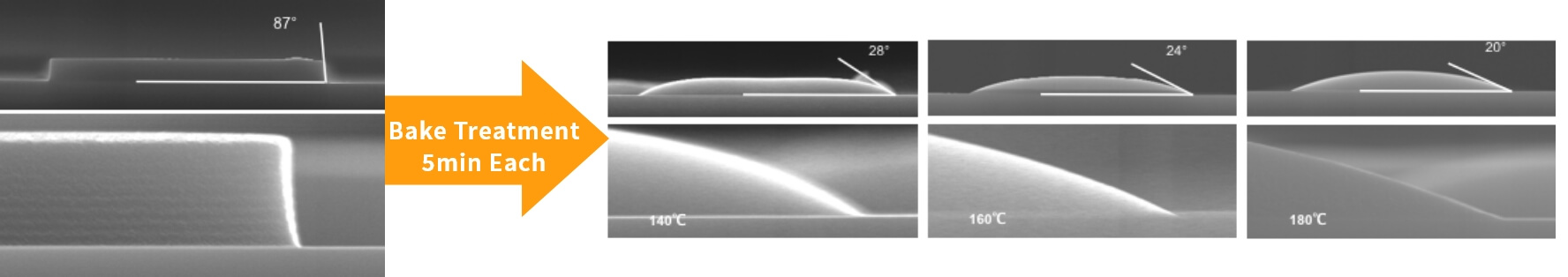
The TMR series has been developed for the application of CIS microlens. This series can be used as a barrier coating layer or as a spherical transparent layer for thermal processing. Characteristics include high transmittance, convex lens shape (thermal flow), and high adhesion to the substrate and transparent structure.
TMR in the text is a pending or registered trademark of TOK.
Thermal Flow Type TMR-P15 PM
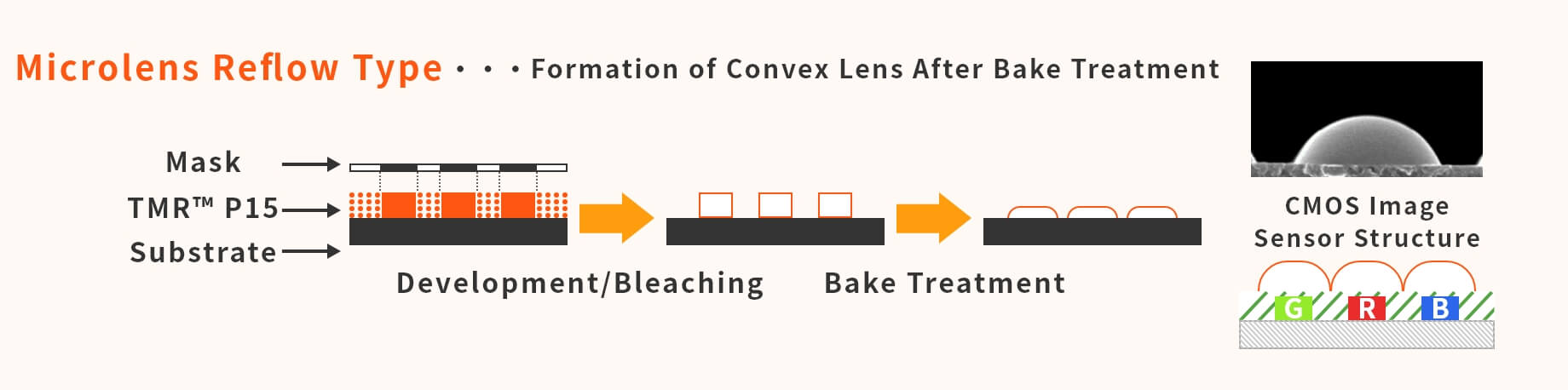
Shape Is Controlled by Heating Process
Measured Transmittance After HST Test
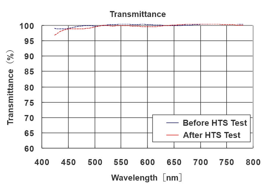
Measurement Sample Preparation Conditions
| Measurement Sample | :TMR-P17 PM |
|---|---|
| Substrate | :1737 glass |
| Film thickness | :0.6um |
| Pre-bake | :90℃, 90sec |
| Bleach Treatment | :100mJ (g-, h-, i-line) |
| 1st Post-bake | :130℃, 5min |
| 2nd Post-bake | :200℃, 5min |
| HTS Test | :250℃, 60min (oven) |
| Wavelength | 400nm | 450nm | 500nm | 550nm | 600nm | 630nm |
|---|---|---|---|---|---|---|
| Before HTS Treatment | 97 | 98 | 99 | 99 | 99 | 99 |
| After HTS Treatment | 95 | 97 | 99 | 99 | 99 | 99 |
Please Feel Free to Contact Us for More Information
For any questions or concerns,
Send an Inquiry Through the Web
Contact Us/Download Information
Please contact us if you have any requests or problems.
You can also access information related to each product.