Tokyo Ohka Kogyo Product Site
DSA Materials

Directed Self Assembly Materials
Directed Self Assembly (DSA) lithography is expected to be the next generation of semiconductor manufacturing technology, as it can be patterned using only coating, annealing, and development. Development of materials utilizing the phenomenon of self assembly of block copolymers (BCP) is underway.
Process Flow
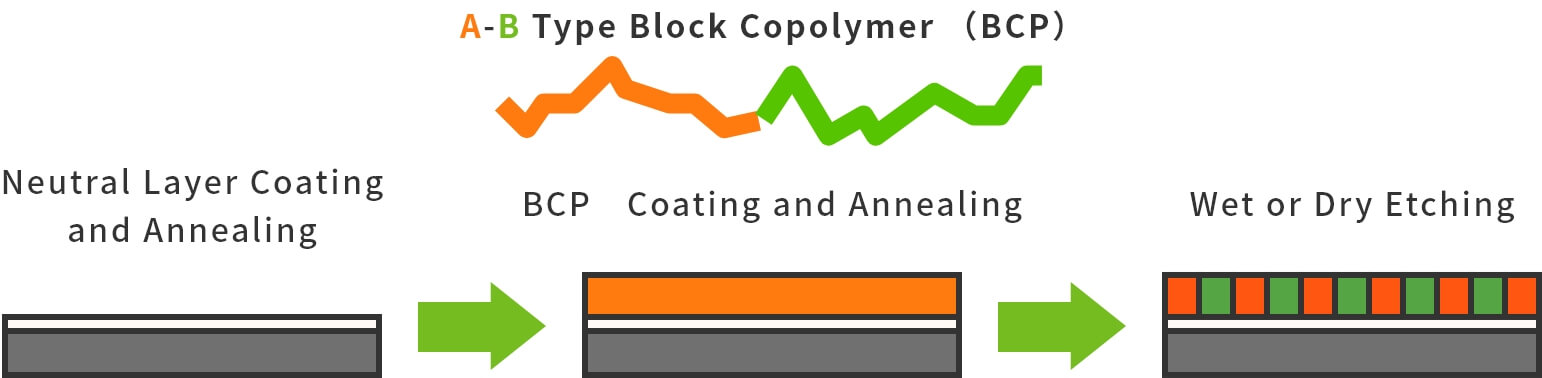
By changing the composition of the BCP, it is possible to form repetitive patterns of lines and holes.
Our target is ~24nm for line/space and ~50nm pitch for holes.
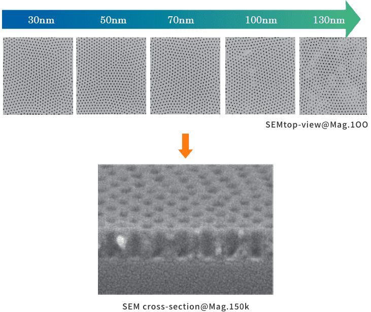
〈 Reference example: BCP with 25nm half-pitch 〉
(Upper Images) Observation results of BCP film with different thickness (30nm~130nm)
(Lower Images) Result of cross-sectional observation with BCP film thickness of 70nm
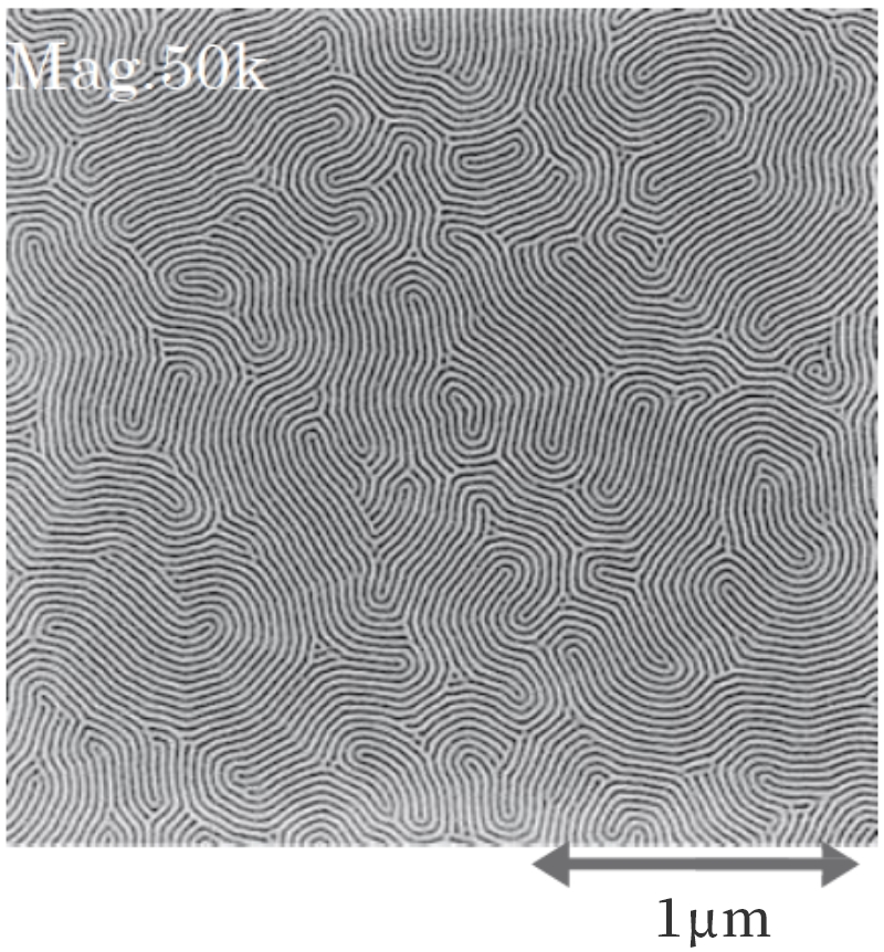
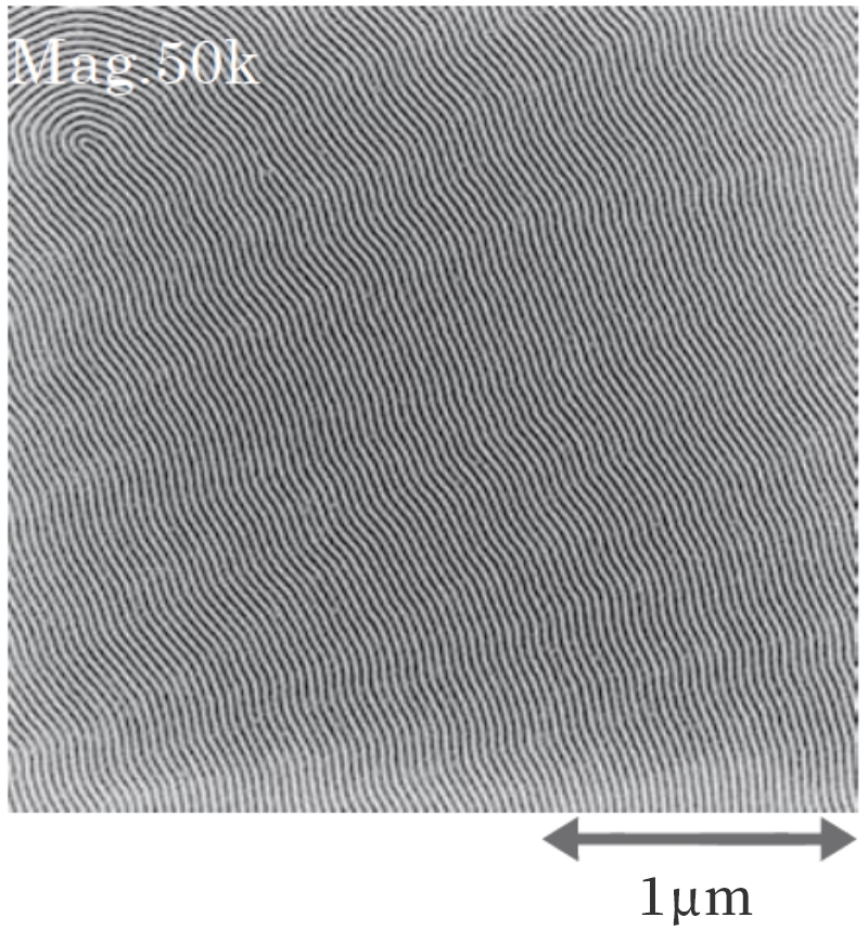
Results of Fingerprint Observation Confirming the Effect of Roughness Improvement of Lamellar Structure
Please Feel Free to Contact Us for More Information
For any questions or concerns,
Send an Inquiry Through the Web
Contact Us/Download Information
Please contact us if you have any requests or problems.
You can also access information related to each product.